Intersubband transitions occurring between quantized electron or hole states confined in quantum wells (QWs) have been the subject of a dealt of studies. In one hand, these studies led to the fabrication of remarkable optoelectronic devices, such as infrared quantum well photodetectors (QWIPs) and quantum cascade lasers (QCLs), operating in a wide energy range, from mid to far infrared frequencies. Most studies have been performed on multi quantum well systems based on III-V compound semiconductors, owing to the possibility these materials offer to grow lattice matched and pseudomorphic heterostructures of very high quality with a variety of energy band alignments and offsets. It would be very interesting to expand this research field to Si-based material. In particular, n-doped compressively-strained Ge (sGe) QWs confined between Ge-rich Si1-yGey barriers (y>0.7) are of special interest for the realization of terahertz devices. In such system the minimal energy electron subbands are located at the L-point of the Brillouin zone, with electron effective masses similar to those typical of III-V compounds and thus with similar intersubband oscillator strengths .
We investigate high quality sGe/Si0.2Ge0.8 multi quantum well structures grown by UHV-CVD on reverse Si0.15Ge0.85/Si(001) virtual substrates. Structural measurements show that wells and barriers are lattice matched. NIR absorption measurements exhibit well defined interband HH1–cG1, LH1–cG1 and HH2–cG2 transition peaks, typical of confined excitons, pointing to a type I band alignment profile.
The
intersubband
recombination dynamics is investigated by means of FEL pump and probe
measurements.


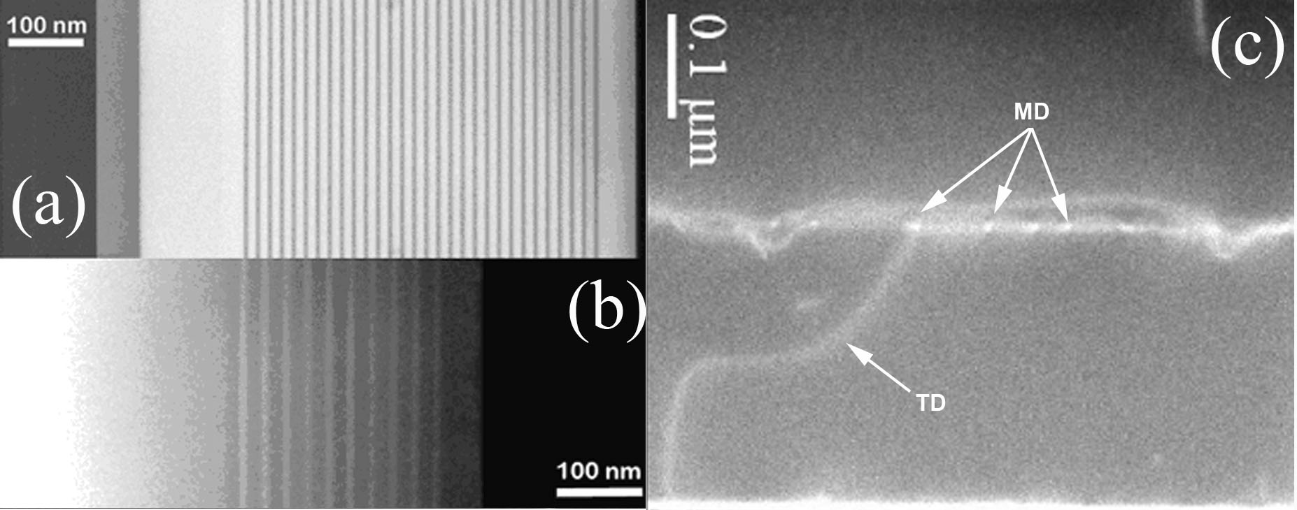
Strained Ge is a promising material both for electronic and optoelectronic applications and its monolithic integration in Si microelectronics is highly desirable. The amount of strain impacting the electronic and optical properties can be tuned upon deposition of the Ge layer on suitably designed SiGe virtual substrates (VS). Among many other VS, the use of reverse graded SiGe VS (RGVS) has recently been proposed. In such structures a thick, relaxed Ge heteroepitaxial layer is first deposited on a Si(001) substrate. Subsequently, the desired in-plane lattice parameter for the Ge epilayer growth is achieved upon decreasing the Ge content x in a sequence of Si1−xGex layers in which the strain is relaxed via the insertion of misfit dislocations. It is therefore of paramount importance to understand the plastic relaxation mechanisms of the virtual substrate governing the dislocation formation and evolution. We have thoroughly investigated the structural properties of RGVS deposited by UHV-CVD. Upon combining XRD, TEM and Raman techniques we have studied the relaxation mechanism end the defect formation occuring in this system.